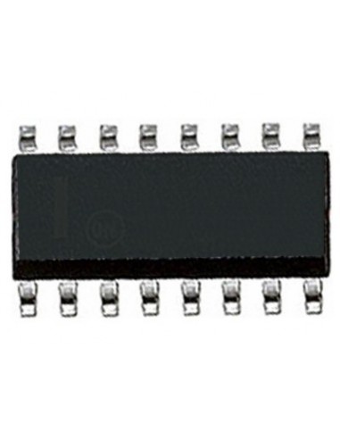
MC14511B BCD−To−Seven Segment Latch/Decoder/Driver
search
  • MC14511B BCD−To−Seven Segment Latch/Decoder/Driver
  • MC14511B BCD−To−Seven Segment Latch/Decoder/Driver
  • MC14511B BCD−To−Seven Segment Latch/Decoder/Driver
  • MC14511B BCD−To−Seven Segment Latch/Decoder/Driver

MC14511B BCD−To−Seven Segment Latch/Decoder/Driver

€1.00
Tax included

MC14511B BCD−To−Seven Segment Latch/Decoder/Driver

Volume discounts

Quantity Unit discount You Save
10 €0.10 €1.00
Quantity

MC14511B
BCD−To−Seven Segment
Latch/Decoder/Driver
The MC14511B BCD−to−seven segment latch/decoder/driver is
constructed with complementary MOS (CMOS) enhancement mode
devices and NPN bipolar output drivers in a single monolithic structure.
The circuit provides the functions of a 4−bit storage latch, an 8421
BCD−to−seven segment decoder, and an output drive capability. Lamp
test (LT), blanking (BI), and latch enable (LE) inputs are used to test the
display, to turn−off or pulse modulate the brightness of the display, and
to store a BCD code, respectively. It can be used with seven−segment
light−emitting diodes (LED), incandescent, fluorescent, gas discharge,
or liquid crystal readouts either directly or indirectly.
Applications include instrument (e.g., counter, DVM, etc.) display
driver, computer/calculator display driver, cockpit display driver, and
various clock, watch, and timer uses.
Features
http://onsemi.com
MARKING
DIAGRAMS
16
PDIP−16
P SUFFIX
CASE 648
16
MC14511BCP
AWLYYWWG
1
1
16
14511BG
AWLYWW
1
16
14511B
AWLYYWWG
Low Logic Circuit Power Dissipation
High−Current Sourcing Outputs (Up to 25 mA)
Latch Storage of Code
Blanking Input
Lamp Test Provision
Readout Blanking on all Illegal Input Combinations
Lamp Intensity Modulation Capability
Time Share (Multiplexing) Facility
Supply Voltage Range = 3.0 V to 18 V
Capable of Driving Two Low−power TTL Loads, One Low−power
Schottky TTL Load, or Two HTL Loads Over the Rated Temperature
Range
Chip Complexity: 216 FETs or 54 Equivalent Gates
Triple Diode Protection on all Inputs
Pb−Free Packages are Available*
MAXIMUM RATINGS
(Voltages Referenced to V
SS
) (Note 1)
Symbol
V
DD
V
in
I
P
D
T
A
T
stg
I
OHmax
P
OHmax
Parameter
DC Supply Voltage Range
Input Voltage Range, All Inputs
DC Current Drain per Input Pin
Power Dissipation,
per Package (Note 2)
Operating Temperature Range
Storage Temperature Range
Maximum Output Drive Current
(Source) per Output
Maximum Continuous Output Power
(Source) per Output (Note 3)
Value
−0.5
to +18.0
−0.5
to V
DD
+ 0.5
10
500
−55
to +125
−65
to +150
25
50
Unit
V
V
mA
mW
°C
°C
mA
mA
SO−16
D SUFFIX
CASE 751B
SO−16
DW SUFFIX
CASE 751G
1
16
MC14511B
ALYWG
1
SOEIAJ−16
F SUFFIX
CASE 966
A
WL, L
YY, Y
WW, W
G
= Assembly Location
= Wafer Lot
= Year
= Work Week
= Pb−Free Package
ORDERING INFORMATION
See detailed ordering and shipping information in the package
dimensions section on page 7 of this data sheet.
*For additional information on our Pb−Free strategy
and soldering details, please download the
ON Semiconductor Soldering and Mounting
Techniques Reference Manual, SOLDERRM/D.
1. Maximum Ratings are those values beyond which damage to the device
may occur.
2. Temperature Derating:
Plastic “P and D/DW” Packages: – 7.0 mW/°C From 65°C to 125°C
3. P
OHmax
= I
OH
(V
DD
V
OH
ELCMC14511B
25 Items
New

You might also like